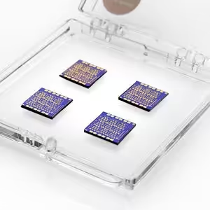
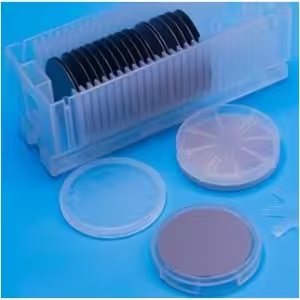
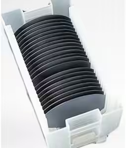
GOFET for Sensing applications
Call for Price
- Growth method: CVD synthesis
- Polymer assisted transfer
- Chip dimensions: 10 mm x 10 mm
- Chip thickness: 675 μm
- Number of GFETs per chip: 27
- Gate oxide thickness: 90 nm
- Gate oxide material: SiO2
- Resistivity of substrate: 1-10 Ω.cm
- Metallization: Au contacts
- Average channel thickness: ≈ nm
Related products
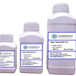
Micronpowder
Price range: ₹5,000 through ₹18,000
This product has multiple variants. The options may be chosen on the product page
Sale!
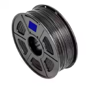
3D Printing Filament
Original price was: ₹28,000.₹25,960Current price is: ₹25,960.
Price range: ₹2,301 through ₹3,894
This product has multiple variants. The options may be chosen on the product page
Sale!
Metal Nanopowder
Price range: ₹3,500 through ₹13,000
This product has multiple variants. The options may be chosen on the product page
Elemental Nanopowder
Price range: ₹4,500 through ₹10,500
This product has multiple variants. The options may be chosen on the product page
Sale!
Sale!
Elemental Nanopowder
Price range: ₹4,500 through ₹9,500
This product has multiple variants. The options may be chosen on the product page
Sale!
Metal Oxide Nanopowder
Price range: ₹1,700 through ₹7,000
This product has multiple variants. The options may be chosen on the product page