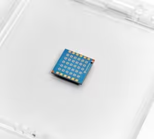
GFET-S31 for Sensing applications
Call for Price
- Growth method: CVD synthesis
- Polymer assisted transfer
- Chip dimensions: 10 mm x 10 mm
- Chip thickness: 525 μm
- Number of channels per chip: 30
- Gate oxide thickness (EOT): 20 nm
- Gate oxide material: Al2O3
- Dielectric breakdown: >13kV/mm
- Metallization: Au Contacts
- Graphene field-effect mobility: > 600 cm2/V.s
- Dirac point: < 5 V
- Yield: > 75 %

