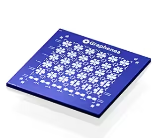
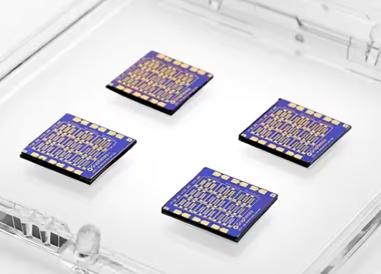
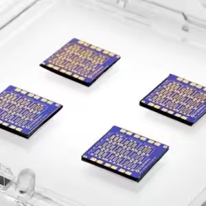
GFET-S10 for Sensing applications
Call for Price
TYPICAL SPECIFICATIONS
- GFET-S10 (Die size 10 mm x 10 mm)
- Processed in Clean Room Class 1000
- Growth method: CVD synthesis
- Polymer assisted transfer
- Chip dimensions: 10 mm x 10 mm
- Chip thickness: 675 μm
- Number of GFETs per chip: 36
- Gate oxide thickness: 90 nm
- Gate oxide material: SiO2
- Dielectric Constant of the SiO2 layer: 3.9
- Resistivity of substrate: 1-10 Ω.cm
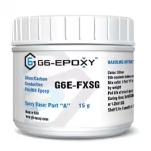
Related products
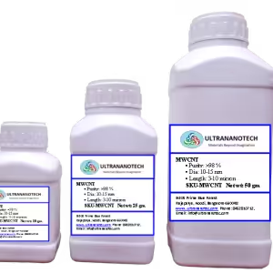
Carbon Nanotubes
Price range: ₹3,500 through ₹16,000
This product has multiple variants. The options may be chosen on the product page

Graphene Oxide Nano
Price range: ₹3,500 through ₹15,300
This product has multiple variants. The options may be chosen on the product page

Out of stock
Graphene Oxide Nano
Price range: ₹2,500 through ₹11,000
This product has multiple variants. The options may be chosen on the product page