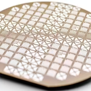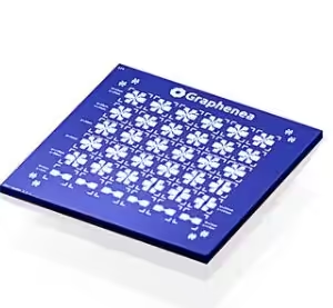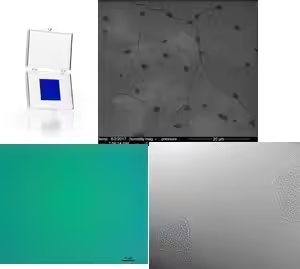
GFET-S20 for Sensing applications
Call for Price
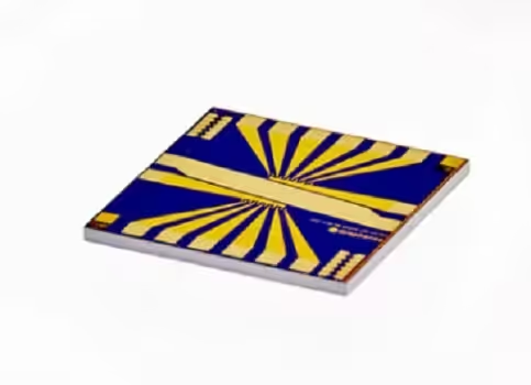
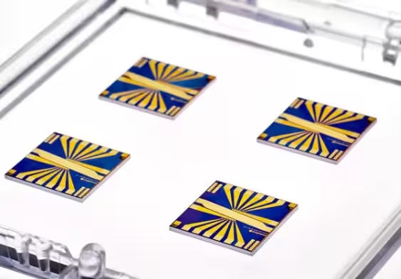
- GFET-S20 (Die size 10 mm x 10 mm)
- Processed in Clean Room Class 1000
- Growth method: CVD synthesis
- Polymer assisted transfer
- Chip dimensions: 10 mm x 10 mm
- Chip thickness: 675 μm
- Number of GFETs per chip: 12
- Gate oxide thickness: 90 nm
- Gate oxide material: SiO2
- Resistivity of substrate: 1-10 Ω.cm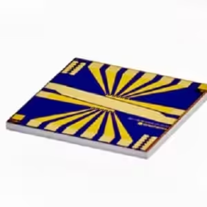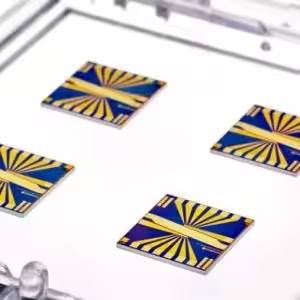
Related products