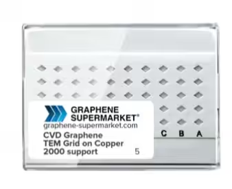
Graphene on Copper 2000 TEM Grids
Call for Price
- CVD Graphene film deposited on Copper TEM grids (2000 Mesh).
- We use CVD graphene grown on Ni to prepare TEM grids
- Thickness of CVD Graphene film: 0.3-2 nm (1-6 monolayers)
- Typical graphene coverage: 60-90%
- CVD Graphene film deposited on Copper TEM grids (2000 Mesh).
- We use CVD graphene grown on Ni to prepare TEM grids
- Thickness of CVD Graphene film: 0.3-2 nm (1-6 monolayers)
- Typical graphene coverage: 60-90%
| QTY | 5 pack, 25 pack |
|---|
Related products
Sale!

Metal Oxide Nanopowder
Price range: ₹1,650 through ₹7,000
This product has multiple variants. The options may be chosen on the product page
Sale!

Metal Oxide Nanopowder
Price range: ₹1,700 through ₹7,000
This product has multiple variants. The options may be chosen on the product page
Sale!
Metal Nanopowder
Price range: ₹3,000 through ₹8,500
This product has multiple variants. The options may be chosen on the product page

Out of stock
Sale!
Elemental Nanopowder
Price range: ₹4,500 through ₹9,500
This product has multiple variants. The options may be chosen on the product page
Sale!

Metal Nanopowder
Price range: ₹8,300 through ₹33,000
This product has multiple variants. The options may be chosen on the product page