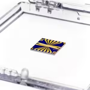
GFET-S20P for Sensing applications
Call for Price
- Growth method: CVD synthesis
- Polymer assisted transfer
- Chip dimensions: 10 mm x 10 mm
- Chip thickness: 525 μm
- Number of GFETs per chip: 12
- Gate oxide thickness: 90 nm
- Gate oxide material: SiO2
- Resistivity of substrate: 1-10 Ω.cm
- Metallization: Au contacts
- Graphene field-effect mobility: >1000 cm2/V.s
- Encapsulation: ≈200 nm glutarimide-based
- Dirac point (liquid gating): <1V
- Minimum working devices: >75 %
Related products
Sale!
Micronpowder
Price range: ₹8,000 through ₹36,000
This product has multiple variants. The options may be chosen on the product page
Sale!
Micronpowder
Price range: ₹4,956 through ₹14,750
This product has multiple variants. The options may be chosen on the product page
Out of stock
Sale!

Micronpowder
Price range: ₹6,844 through ₹21,830
This product has multiple variants. The options may be chosen on the product page
Sale!
Metal Nanopowder
Price range: ₹3,500 through ₹13,000
This product has multiple variants. The options may be chosen on the product page
Sale!
Boats
Price range: ₹13,000 through ₹14,000
This product has multiple variants. The options may be chosen on the product page
Price range: ₹2,301 through ₹3,894
This product has multiple variants. The options may be chosen on the product page