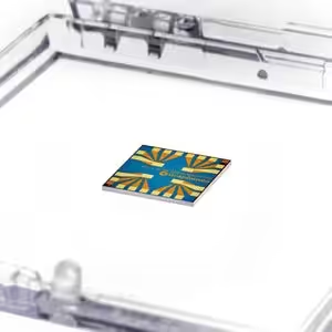
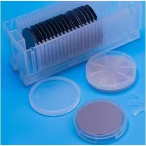
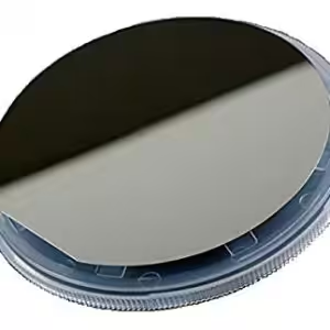
GFET-S22 for Sensing applications
Call for Price
- Growth method: CVD synthesis
- Polymer assisted transfer
- Chip dimensions: 10 mm x 10 mm
- Chip thickness: 675 μm
- Number of GFETs per chip: 12 in parallel
- Gate oxide thickness: 90 nm
- Gate oxide material: SiO2
- Resistivity of substrate: 1-10 Ω.cm
- Metallization: Au contacts
- Graphene field-effect mobility: >1000 cm2/V.s
- Encapsulation: 50 nm Al2O3
- Dirac point (liquid gating): <1V
- Minimum working devices: >75 %
Related products
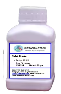
Micronpowder
Price range: ₹4,956 through ₹14,750
This product has multiple variants. The options may be chosen on the product page
Sale!
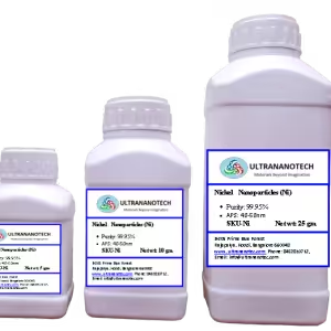
Metal Nanopowder
Price range: ₹3,000 through ₹8,500
This product has multiple variants. The options may be chosen on the product page
Sale!
Sale!

Sale!
Multi Elements Nanopowders
Price range: ₹3,000 through ₹9,000
This product has multiple variants. The options may be chosen on the product page
Sale!
Metal Nanopowder
Price range: ₹3,500 through ₹13,000
This product has multiple variants. The options may be chosen on the product page