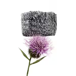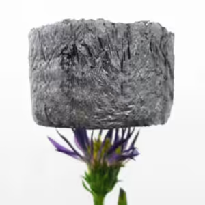
Monolayer Graphene on Cu with PMMA Coating
Call for Price
- Monolayer Graphene on Cu with PMMA Coating – Processed in Clean Room Class 1000
- A single-layer graphene film on a copper substrate. This product is provided with a PMMA coating on top of the Graphene in order ease the transfer process and to avoid contamination. It’s a high quality product, with a great homogeneity.
| Size |
|---|
Related products
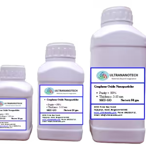
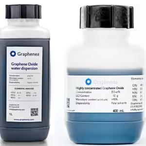
Graphene Oxide Nano
Price range: ₹3,500 through ₹15,300
This product has multiple variants. The options may be chosen on the product page