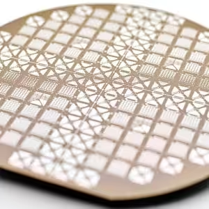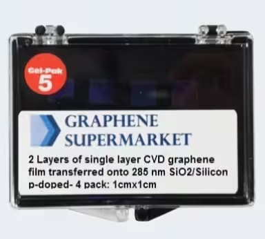
Two Layers of CVD Graphene Film on SiO2/Si Wafer
Call for Price
- Two layers of single layer CVD graphene films are transferred onto 285 nm p-doped SiO2/Si wafer
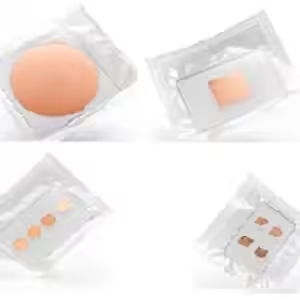
- Size: 1cmx1cm; 8 pack
- Each graphene film is transferred consecutively onto the wafer
- The thickness and quality of our graphene film is controlled by Raman Spectroscopy
- The graphene coverage of this product is about 98%
- The graphene film is continuous, with minor holes and organic residues
- Each graphene film is predominantly single layer (more than 95%) with occasional small multilayer islands (less than 5% bi-layers)
- Each graphene film is polycrystalline, i.e. it consists of grains with different crystallographic orientation
- There is no A-B stacking order. The graphene films are randomly oriented with respect to each other
- Sheet Resistance: 215-700 Ω/square
- Two layers of single layer CVD graphene films are transferred onto 285 nm p-doped SiO2/Si wafer
- Size: 1cmx1cm; 8 pack
- Each graphene film is transferred consecutively onto the wafer
- The thickness and quality of our graphene film is controlled by Raman Spectroscopy
- The graphene coverage of this product is about 98%
- The graphene film is continuous, with minor holes and organic residues
- Each graphene film is predominantly single layer (more than 95%) with occasional small multilayer islands (less than 5% bi-layers)
- Each graphene film is polycrystalline, i.e. it consists of grains with different crystallographic orientation
- There is no A-B stacking order. The graphene films are randomly oriented with respect to each other
- Sheet Resistance: 215-700 Ω/square
Related products