ULTRANANOTECH, Uncategorized
Silicon wafer and Its Application
22
Feb
Feb
Silicon has property in between metal and nonmetal and hence it is called metalloid. Silicon is the most abundant element in nature. Silicon wafers are made from a single crystal of highly pure silicon, typically with less than one part per billion of contaminants. The Czochralski (CZ) process is the most common method of forming large crystals of this purity, which involves pulling a seed crystal from molten silicon, commonly known as a melt. The seed crystal is then formed into a cylindrical ingot known as a boule. The other method of single crystal silicon growth process is known as Float zone silicon (FZ).
The most common dimensions of silicon wafers depend on their application. The wafers used in ICs are round with diameters typically ranging from 50 to 300 millimeters (mm). The thickness generally increases with the diameter and is usually in the range of 525 to 775 microns (μm). The wafers in solar cells are usually square with sides measuring 100 to 200 mm. Their thickness is between 200 and 300 μm, although this is expected to be standardized to 160 micron in the near future.
Application of Silicon Wafer
Silicon wafer is a thin slice of crystalline silicon commonly used in the electronics industry. Silicon wafers are most often used as the substrate for integrated circuits (ICs), although they’re also a major component in photovoltaic, or solar, cells. The basic process of fabricating these wafers is the same for both of these applications, although the quality requirements are much higher for the wafers used in ICs. These wafers also undergo additional steps such as ion implantation, etching and photolithographic patterning, which aren’t needed for solar cells
Integrated Circuits (IC)
An IC, also known as a microchip or just chip, is a set of electronic circuits set into a substrate of semiconducting material. Monocrystalline silicon is currently the most common substrate for ICs, although gallium arsenide is used in some applications such as wireless communication devices. Wafers made of silicon-germanium alloys are also becoming more widely used, typically in applications where the greater speed of silicon-germanium is worth the higher cost.
ICs are currently used in most electronic devices, having virtually replaced separate electronic components. They’re smaller, faster, and cheaper to manufacture than discrete components. The rapid adoption of ICs in the electronics industry is also due to the modular design of ICs, which easily lends itself to mass production.
Random-access memory (RAM) chips are one of the most common types of ICs, due to their particular need for a high transistor density. The thickness of the layers of photolithographic material in a RAM chip has been shrinking steadily and are now much thinner than the width of the device itself.
These layers are developed in a similar manner to regular photographs except that ultraviolet light is used rather than visible light since the wavelengths of visible light are too large to create features with the necessary precision. The features of modern ICs are so small that process engineers must use electron microscopes to debug them.
IC Fabrication
The fabrication of ICs is a highly automated process that uses many specific techniques. These capabilities drive the high cost of building a fabrication facility, which can exceed $8 billion or more. This cost is expected to increase much more quickly than inflation due to the continuing need for greater automation.
The trend towards smaller transistors will continue for the foreseeable future, with 14 nm was being the state of the art in 2016. IC manufacturers such as Intel, Samsung, Global Foundries and TSMC are expected to begin the transition to 10 nm to 8nm transistors by the end of 2018-2020.
Large wafers provide an economy of scale, which reduces the total cost of ICs. The largest wafers that are commercially available are 300 mm in diameter, with 450 mm expected to be the next maximum size. However, significant technical challenges still exist for making wafers of that big size.
Additional techniques are used in the fabrication of ICs include tri-gate transistors, which Intel have manufactured with a width of 22 nm since 2011. IBM uses a process known as strained silicon directly on insulator (SSDOI), which removes the silicon-germanium layer from a wafer.
Copper is replacing aluminium interconnects in ICs, primarily due to its greater electrical conductivity. Low-K dielectric insulators and Silicon on Insulators (SOIs) are also advanced manufacturing techniques for ICs
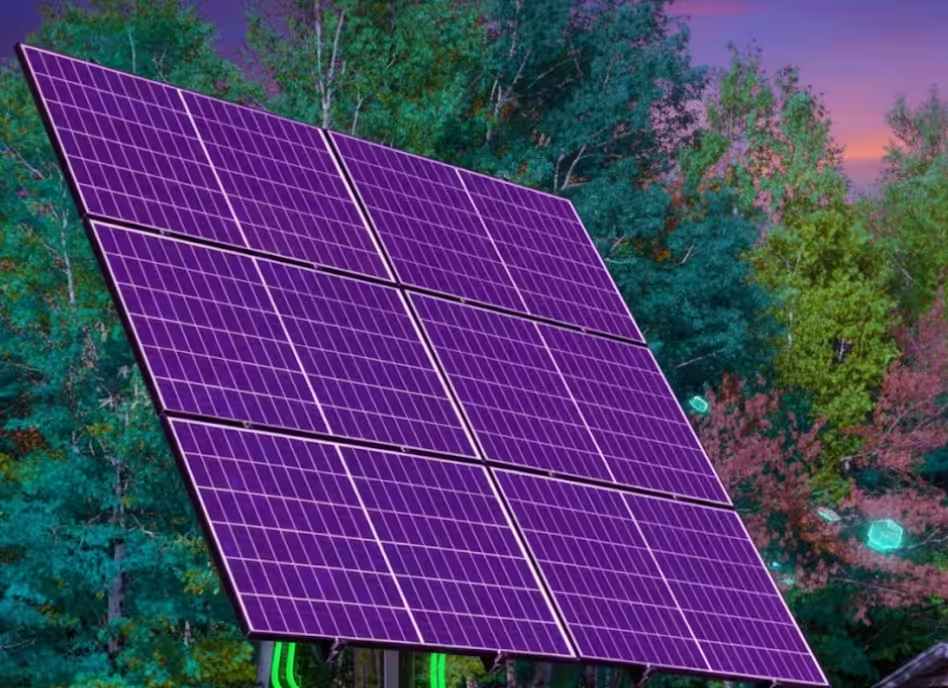
Solar Cells
A solar cell uses the photovoltaic effect to convert light energy into electrical energy, which generally involves the absorption of light by some material to excite electrons into a higher energy state. It’s a type of photoelectric cell, a device that changes its electrical characteristics when exposed to light.
The generation of electricity as an energy source is one of the most well-known applications for solar cells. These types of solar cells use a light source to charge a battery, which can be used to power an electrical device. Solar cells are often integrated into the devices that they’re intended to generate power
Solar cells may be classified into first, second, and third-generation types. First-generation cells are composed of crystalline silicon, including monocrystalline silicon and polysilicon. They’re currently the most common type of solar cell. Second-generation cells use thin film composed of amorphous silicon and are typically used in commercial power stations. Third-generation solar cells use thin-film developed with a variety of emerging technologies and currently have limited commercial applications
COURTESY: ULTRANANOTECH PVT. LTD
For inquiry related to silicon wafer visit us at: https://ultrananotec.com/