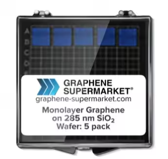
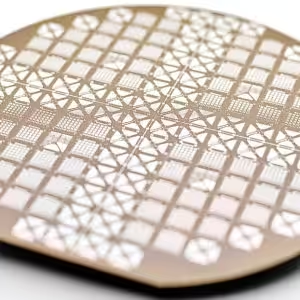
Monolayer Graphene on 90 nm SiO2 Wafer
Call for Price
Properties of Silicon/Silicon Dioxide Wafers:
- Oxide Thickness: 90 nm
- Color: Violet
- Wafer thickness: 525 micron
- Resistivity: 0.001-0.005 Ω⋅cm
- Type/Dopant: P/Boron
- Orientation: <100>
- Front Surface: Polished
- Back Surface: Etched
- RCA cleaned
- The thickness and quality of our graphene films is controlled by Raman Spectroscopy
- The graphene coverage of this product is about 95%
- The graphene film is continuous, with occasional holes and cracks
- Organic and PMMA residues can be observed
- The graphene film is polycrystalline, i.e. it consists of grains with different crystallographic orientation
- Sheet Resistance: 660-1,500 Ω/square
Properties of Silicon/Silicon Dioxide Wafers:
- Oxide Thickness: 90 nm
- Color: Violet
- Wafer thickness: 525 micron
- Resistivity: 0.001-0.005 Ω⋅cm
- Type/Dopant: P/Boron
- Orientation: <100>
- Front Surface: Polished
- Back Surface: Etched
- RCA cleaned
| Size |
|---|
Related products
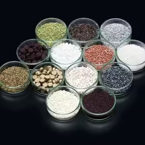
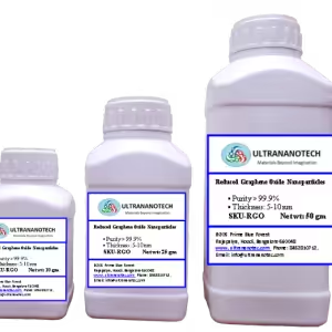
Graphene Oxide Nano
Price range: ₹2,500 through ₹11,000
This product has multiple variants. The options may be chosen on the product page
Graphene Oxide Nano
Price range: ₹3,500 through ₹15,300
This product has multiple variants. The options may be chosen on the product page