Uncategorized
Coated Silicon Wafer
23
Jan
Jan
Introduction
A silicon wafer is a thin, flat disc made from purified silicon. It is the primary substrate for manufacturing integrated circuits (ICs) and semiconductor devices.
A coated silicon wafer is a silicon wafer with one or more layers of materials deposited on its surface.Coating a silicon wafer is not merely an added step; it’s a critical process that enhances performance, protects delicate structures, and makes modern electronics possible.
Manufacturing Process:
Before coatings can be applied, the silicon wafer must first undergo a series of preparation steps to ensure it is free of contaminants and has the appropriate surface characteristics
- The manufacturing process begins with the creation of a silicon ingot, which is typically produced using the Czochralski (CZ) process.
- Once the single crystal silicon ingot is solidified, it is sliced into thin disks called wafers. The diameter of the wafers can range from 25 mm to 300 mm but can vary in size depending on the application.
- The wafers produced through slicing typically have rough surfaces, which need to be smoothed for high-precision applications. The chemical-mechanical polishing (CMP) process is used to smooth the wafer’s surface.
- After polishing, the wafer is thoroughly cleaned to remove any residual chemicals, dust, or particles.The cleaning is done using a series of chemical baths and rinsing with deionized water. The wafers are then dried using a spin-drying process, which uses centrifugal force to remove any excess water.
- Once the silicon wafer has been prepped, the coating application process begins. Different types of coatings are applied depending on the function of the waferlike ARC, CVD, LPCVD, PVD,ALD.
- The wafers undergo rigorous quality control and inspection processes to ensure the coatings are applied uniformly and meet the required specifications.
- The wafers are cleaned one final time to remove any particles or contamination that may have accumulated during the coating and testing process.
- The cleaned wafers are dried using a spin dryer or a nitrogen blow-off to ensure they are completely dry and free of moisture.
- They are packaged in protective containers that prevent physical damage and contamination.
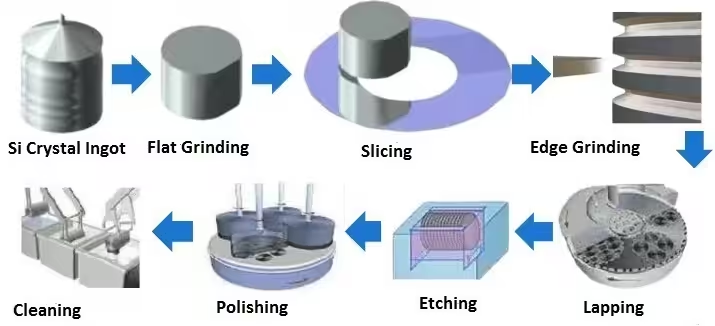
Fig.: Silicon wafer manufacturing process
Types of Coatings:
Optical Coatings:
- Anti-Reflective (AR) Coating: Silicon dioxide (SiO2) or titanium dioxide (TiO2) coating to reduce reflection.
- High-Reflection (HR) Coating: Aluminum oxide (Al2O3) or silver (Ag) coating for high reflectivity.
- Dielectric Mirror Coating: Alternating layers of Silicon dioxide (SiO2) or titanium dioxide (TiO2) for high reflectivity.
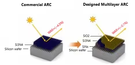
Fig: Showing the antireflective properties after applying coating
Semiconductor/MEMS Coatings:
- Polysilicon (Poly-Si) Coating: For transistor gates, resistors, or capacitors.
- Silicon Nitride (Si3N4) Coating: For insulation, passivation, or diffusion barriers.
- Silicon Oxide (SiO2) Coating: For insulation, passivation, or gate dielectrics.
Conductive/ Metal Coatings:
- Aluminum (Al) Coating: For interconnects, electrodes, or contacts.
- Copper (Cu) Coating: For interconnects, electrodes, or contacts.
- Gold (Au) Coating: For wiring, bonding, or contacts.
Biomedical Coatings:
- Titanium Dioxide (TiO2) Coating: For implantable devices, biosensors, or biochips.
- Hydroxyapatite (HA) Coating: For bone implants, dental implants, or tissue engineering.
Solar Cell Coatings:
- Aluminum Oxide (Al2O3) Coating: For rear surface passivation.
- Silver (Ag) Coating: For front contact metallization.
Why are Coated Silicon Wafers Important?
The use of coated silicon wafers has become indispensable across a variety of industries for several reasons:
Improved Efficiency: Coatings enhance the functionality of silicon wafers, ensuring that devices perform at higher efficiency levels.
Increased Durability: Protective coatings help to extend the lifespan of silicon wafers, reducing the likelihood of failure and the need for frequent replacements.
Cost-Effectiveness: By improving performance and durability, coatings reduce long-term maintenance costs and improve the overall reliability of devices.
Advancement of Technology: Coated wafers are essential for pushing the boundaries of modern electronics, from more powerful processors to more efficient solar cells, supporting the ongoing evolution of technology.
Applications:
Electronics and Semiconductor Industry: Microprocessors, Memory chips (DRAM, Flash), Logic chips, Analog chips, Power management devices, RF devices, Optoelectronic devices (LEDs, photodiodes)
Solar Energy Industry: Solar cells, Photovoltaic modules, Concentrated Photovoltaic (CPV) systems
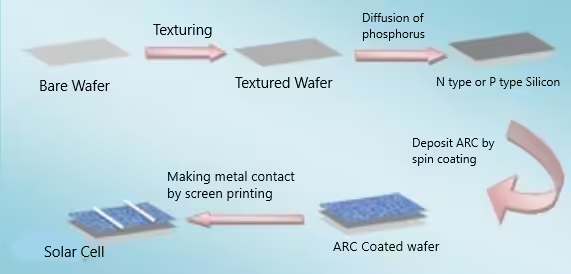
Fig: Showing the application of coated silicon wafer in solar cell
Optical and Photonics Industry: Optical fibers, Optical communication systems, Laser diodes, Photodetectors, Optical sensors
Biomedical and Healthcare Industry: Biosensors, Biochips, Medical implants (pacemakers, prosthetics), Diagnostic devices, DNA microarrays
MEMS and Sensor Industry: Accelerometers, Gyroscopes, Pressure sensors, Temperature sensor, Inertial Measurement Units (IMUs)
Automotive and Aerospace Industry:Navigation systems, Radar systems, Advanced driver-assistance systems (ADAS), Satellite communications
Consumer Electronics Industry:Smartphones, Tablets, Laptops, Smartwatches, Gaming consoles
Other Applications: Flat panel displays, LED lighting, Water purification systems, Air quality monitoring systems, Industrial control systems
Coated silicon wafers are used in various forms, including:
- Bare wafers
- Patterned wafers
- Metallized wafers
- Dielectric-coated wafers
- Polymer-coated wafers
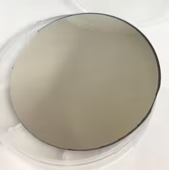
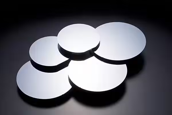
Fig: Platinum coated silicon wafer
Challenges faced to manufacture coated silicon wafer
- Uniformity and thickness control
- Adhesion and interface quality
- Defect density and contamination
- Scalability and cost-effectiveness
- Integration with other materials and processes
Innovations in the industry
- Atomic Layer Deposition (ALD) for ultrathin coatings
- 3D printing for complex coating structures
- Nanomaterials for enhanced coating properties
- Plasma-enhanced CVD for improved uniformity
- Automated coating systems for increased efficiency
Conclusion
Coated silicon wafers are a crucial component in the production of microelectronic, solar, and optoelectronic devices. The type of coating used depends on the specific application and the desired properties of the device. Coated silicon wafers offer improved performance, increased efficiency, and enhanced functionality, making them an essential material in the development of advanced technologies.
Courtesy: Dr. Subhadeep and Simran, Sales Executive at Ultrananotech Pvt Ltd